Analog circuits: An analog circuit is a circuit with continuous,
variable signal (i.e. an analog
signal) as resist or opposed to a digital circuit where a
signal must be one of two discrete levels. Analog circuits within electrical equipment can convey/
carries information through changes in the current, voltage, (or) frequency.
In analog circuits we have two types. Those
are
1.
DC analysis
2.
AC analysis
Ac analysis is again
sub-divided into two types. Those are
1.
Low frequency analysis
2.
High frequency analysis
While performing these
analog circuit analysis problems we have to remember these following important
points.
DC analysis:
1. find out VCE, IC. because these are operating points of a transistor in a DC analysis.
2. In DC analysis we
make all ac input signals to zero.
3. All external
capacitors are open circuited in DC analysis.
4. Amplifies operates
in active region
5. Apply KVL, KCL to
obtain the operating points of amplifier.
AC analysis:
In AC analysis is
required to obtain gain, input resistance, output resistance and frequency of
operation.
1. in Ac analysis we
make all DC sources to zero.
2. All external
capacitors are short-circuited.
3. in low frequency
analysis transistor is replaced by its low frequency small signal model.
4. in high frequency
analysis transistor is replaced by its high frequency small signal model.
5. After these
following steps now we will apply to the KCL, KVL to obtain gain, input output
resistance and frequency response of amplifiers.
Before learning AC analysis of transistor now
we will see basics of hybrid parameters and its diagrams.
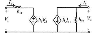
Hybrid parameter two-port network:
With the help of
hybrid parameters we will find input, output voltages & currents using
these two equations.
V1 = h11I1
+ h12V2
I2= h21I1 + h22V2
h11= V1/I1 (at V2 =0) this is input resistance with o/p short-circuit
h12= V1/V2
(at I1=0) reverse
voltage gain with i/p open-circuit
h21 = I2/I1 (at V2=0) forward current gain with o/p short-circuit
h22 = I1/V2 (at I1=0) output conductance with i/p open-circuit
Transistor Low
Frequency Hybrid model:
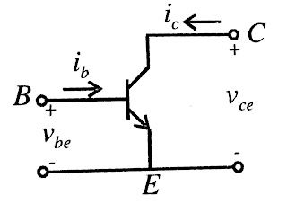
Transistor can be considered as two port
network, one is input port and one is output port. Input is applied to the
input port and output is taken from output port of hybrid networks.
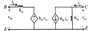
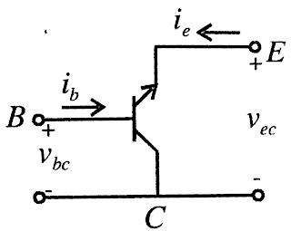
The transistor configurations and their hybrid model shown in below.
Euqtion for the CE hybrid model is
Vbe = hieib + hreVce
Ic = hfeib + hoeVce
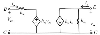
Euqtion for the CC hybrid model is
Vbc = hicib + hrcVec
Ie = hfcib + hocVec
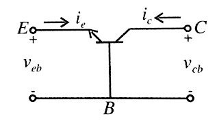
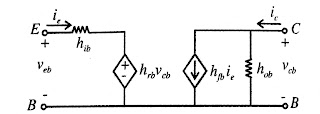
Euqtion for the CB
hybrid model is
Veb = hibie + hrbVcb
Ic = hfbie
+ hobVcb
Analysis of two port network
Here we dicuss the
hybrid model of two port network which is connected to source resistance Rs
and source voltage Vs at input port and output port is connected to
load resistor RL as shown in below fig.
Current gain
AI = I0/I1
From the output loop
we can see that I0 = -I2
Applying KVL in the output loop
(-1/h22) (i2-h21I1)
+ I0RL=0
Replacing –I2=I0
(I0/h22) + I1(h21/h22)+I0RL=0
AI=I0/I1 = -h21/(1+h22RL)
Input resistance:
Ri =
Vi/Ii
From input loop we will get
From input loop we will get
V1 - h11I1 -h12V2=0 -----------------(1)
V2=I0RL
Substituting I0=AII1
V2=AII1RL
Therefore the equation (1) of input loop is
V1 - h11I1 -h12 AII1RL =0
Ri = h11 +
h12AIRL
Voltage gain:
Av=v2/v1
= AII1RL/ RiI1
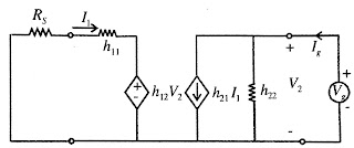
Applying kvl at this output loop is
Vg=(1/h22)(Ig-h21I1)
From the input loop
-(Rs + h11)I1 – h12V2=0
In input loop we substitute V2=Vg
-(Rs + h11)I1 – h12Vg=0
(Rs + h11)I1 = - h12Vg
I1 = -( h12Vg/Rs+h11)
Then I1 substitute in the output loop quation
Vg=(1/h22)(Ig-h21(-(
h12Vg/Rs+h11)))
Vg=(1/h22)(Ig + h21h12Vg
/ Rs+h11)
h22Vg= Ig + h21h12Vg
/ Rs+h11
Ig= h22Vg – ( h21h12Vg / Rs+h11)
Ig= h22Vg – ( h21h12Vg / Rs+h11)
Y0 = Ig/Vg = h22-(h12h21/Rs+h11)
R0= 1/Y0

