1. A
Bipolar Transistor is Operating in the active region with a collector current
of 1mA. Assuming that the β of the transistor is 100 and the thermal Voltage (Vt)
is 25mV,the trans conductance(gm) and the input resistance (rπ)
of the transistor in the common emitter Configuration, are
A. gm
= 25mA/V & rπ =15.625KOhm
B. gm
= 40mA/V & rπ = 4.0KOhm
C. gm
= 25mA/V & rπ = 2.5KOhm
D. gm
= 40mA/V & rπ = 2.5KOhm
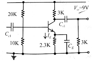
2. In the Following transistor Circuit,VBE=0.7V
and re= 25mV/IE ,and β large all the capacitance's are very Large
.
A.1mA
B.2mA
C.5mA
D.10mA
The mid -band voltage gain of the
amplifier is approximately
A. -180
B. -120
C. -90
D. -60
3.The
Transistor amplifier shown in figure is biased with a current source I and has a very large β the value of C is very large .VBE
=0.7V ,T=300 K
1.The DC Collector Voltage is
A. 1V
B.
2V
C.3V
D. 4V
2. The low Frequency small signal Voltage
Gain Av=vo/vi is
A. 40
B. 80
C.
120
D.
160
4.
A Small signal source Vi(t) =
A cos 20t+ B sin 10^6t is applied to a transistor amplifiers as shown below.
The transistor has β =150 and hie=3kohm .Which expression best
approximates vo (t)?
A. Vo ( t) = -1500 (A cos 20t + B sin 10^6 t )
B.
Vo ( t) = -150 (A cos 20t + B sin 10^6 t
)
C.
Vo ( t) = -1500 B sin 10^6 t
D.
Vo ( t) = -150 B sin 10^6 t
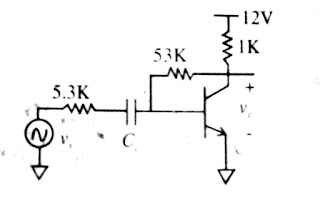
5. In the Transistor amplifier circuit shown
in the figure below ,the transistor has the Following . parameters
βDc=60,Vbe
=0.7V,hie à
infinity,hfe à
infinity.The capacitance CC can be assumed to be infinite. In the figure above ,the ground has been shown by the symbol
1.Under
the DC conditions ,the collector -to- emitter Voltage drop is
A. 4.8
Volts
B. 5.3
Volts
C.
6.0 Volts
D. 6.6 Volts
2. If BDC is increased by 10% ,the collector
-to-emitter Voltage drop
A. Increases by less than or equal to 10%
B. Decreases by less than or equal to 10%
C. Increases by More than 10%
D. Decreases by More than 10%
3.
The small signal gain of the amplifier Vc/Vs is
A. -10
B. -5.3
C. 5.3
D. 10
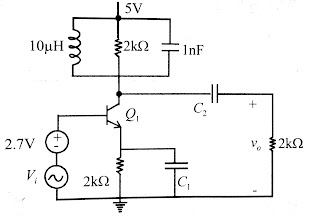
6.In
the Circuit shown below , capacitors C1 and C2 are very large and are short at
the input frequency . Vi is a small signal input.The gain magnitude |vo/vi| at
10 Mrad/s is
A.
Maximum
B.
Minimum
C.
Unity
D.
Zero
7.The
current ib through the base of a
silicon npn transistor is 1+0.1cos (10000πt)mA.At 300 K, the rπ
in the small signal model of the transistor is
A.
250ohm
B.
27.5ohm
C.
25ohm
D.
22.5ohm
8.The
Voltage gain Av of the circuit shown below is
A.|Av|~ 200
B.
|Av|~100
C.
|Av|~20
D.
|Av| ~1p
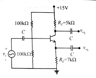
9.Consider
the amplifier circuit shown in figure where β of transistor is very large ,Vbe=0.7V,T=300K,C
is very large
1.The
low frequency small signal voltage gain Vo1/Vs is
A.0.491
B.0.682
C. 0.902
D. 0.996
2.
The low frequency small signal voltage gain Vo2/Vs is
A. -0.711
B. -71.1
C. 0.711
D. 71.1
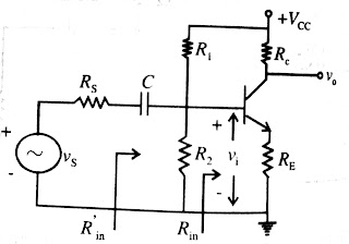
10.The
Transistor amplifier circuit is shown in figure.C is coupling capacitor
1.The
input Resistance Vin of the amplifier is
A. (re
+RE)
B re+Re /1+hfe
C. (1+hfe)(re+RE)
D. re
2.
The voltage gain A=Vo/Vi of the amplifier is
A.
-hfe Rc/(1+hfe)(re+RE)
B.
–(1+hfe)RC/hfe re
C.
–(re+RE)/hfe RE)
D.
–re / ( 1+hfe)Rc
3.
If a bypass capacitor is used between emitter and ground then the voltage gain
is approximately equal to
A.
–re /RC
B.
–re Rc
C. -Rc/re
