PN-Junction
Diode | PN-junction Diode Definition, Working, Characteristics
PN-junction is formed when an N-type material is fused or added
together with a P-type material
creating a semiconductor diode.the below fig show the PN Junction diode symbol.
Formation of PN-Junction Diode
For
making PN-Junction Diode we should
take two semiconductors. One is P-type and one is N-type semiconductors which
have good doping concentration for conduction. So, before knowing formation of PN-junction
diode let us we can know little basic of P and N-type semiconductors.
 |
| P-Type Semiconductor |
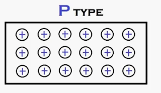
The above fig shows
the P-type semiconductor material which is used for one semiconductor piece of PN Junction Diode. So many peoples are thinking that p-type
semiconductor has large number of holes & current conduction is due to
these holes only. This causes the total electric charge of p-type semiconductor
is positive. But their thinking is wrong. Because p-type semiconductor has
larger number of holes, but those holes are provided by the trivalent atoms (trivalent
Impurity added to pure semiconductor) that are electrically neutral. So, the
total electric charge of p-type semiconductor is also neutral.
 |
| N-type Semiconductor |
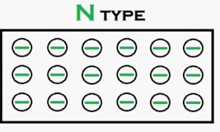
The above fig shows
the N-Type semiconductor material. N-Type semiconductor is generated
by adding (Doping) pentavalent impurities
like (phosphorus) P, As (Arsenic), Sb (antimony) etc… Generally pentavalent impurity is called donors because those pentavalent atoms
are ready to give free electrons to semiconductors. The impurities are
called dopants. The purpose of doing
this is to make a high charge carriers or electrons available in the materials for getting
more conduction. In N-type semiconductors the no. of electrons are more than the
no. of holes, so electrons are measured as majority charge carriers and holes
are referred to as minority charge carriers. And also N-type
semiconductor is also electrically
neutral.
When
we add or fuse the both P and N types semiconductors it forms a PN-Junction diode. This PN-Junction
diode have small deletion
region layer that is shown in below fig.
Small Depletion
Region Junction
The electrons and
holes are near the junctions these charge carriers are jumped. i.e. the holes
in P-side semiconductor which are near to junction are jumped from P region to
N region and also electrons are jumped from N region to P region.
 |
| Movement of Electrons & Holes |
This will cause to
increase the depletion region. And it would be create depletion region or space
charge region. In this space charge
region immobile charge carriers are present .these immobile charge carriers does
not have charge.
Forward Bias condition of PN-Junction Diode
 |
| PN-Junction Diode Forward Bias |
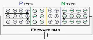
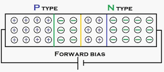
Forward
Bias condition of PN-Junction diode is nothing but connecting positive terminal
of battery to P-type semiconductor material of PN-Junction diode and
negative terminal of battery is connecting to the N-type semiconductor of PN-Junction
diode. This will cause the charge carriers which resides in P & N
type semiconductor bars of PN-Junction diode are gain some more energy. This
will cause the charge carriers cross to barrier potential and the width of
barrier potential of PN-Junction diode
is reduced as shown in below.
If the voltage in the forward bias is
above the specific range the electrons in N region drafts through the PN-Junction and migrates to the P
region and the holes in the P region drafts through the junction and migrates
to the N region.
Reverse
Bias Condition Of PN-Junction Diode:
 |
| Reverse biased PN Junction Diode |
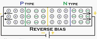
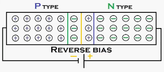
Reverse
Bias condition of PN-Junction Diode is
nothing but connecting positive terminal of battery to N-type semiconductor of PN-Junction
diode and negative terminal of battery is connecting to the P-type
semiconductor of PN-Junction diode.
This will cause to when we applied to reverse
bias voltage PN-Junction diode. Holes
in P region of PN-Junction diode
is attracted to negative terminal of
battery and electrons in N region of PN-Junction diode is attracted to the positive
terminal of battery. Because of unlike charges are attract each other. This will
cause to increases the space charge region or depletion region of PN-Junction
diode.
Whenever the reverse bias voltage reached
to particular specified voltage of PN-Junction diode with stand then it would be
break the avalanches break down and large current flows through the PN junction diode and it may causes to destroy or damage the PN
junction diode.
Characteristics
of PN Junction Diode
PN Junction Diode has two operating regions and three possible biasing conditions
for the standard PN Junction Diode.
They are:
Zero Bias – In this case no external voltage
potential is applied to the PN junction diode.
Reverse Bias – In this region of operation
voltage potential is connected (-ve) negative to the P-type material and (+ve) positive
to the N-type material across the diode which has the effect of increases the PN junction diode’s
width.
Forward Bias – In this region of operation voltage
potential is connected (+ve) positive to the P-type material and (-ve) negative
to the N-type material across the diode which has the effect of decreasing the PN junction diodes width.
Zero Biased PN Junction Diode
In the
zero bias junctions, potential provides higher potential energy to the holes on
the P side and N side terminals. When the terminals of the junction diode are
shorted, few majority charge carriers in the P-side with enough energy to
overcome the potential barrier to travel across the depletion region.
Therefore, with the help of majority charge carriers, the current starts to flow
in the diode and it is noted to as forward current. The minority charge
carriers in the N-side move across the depletion region in reverse direction
and it is referred to as reverse current
Reverse Biased PN Junction Diode
When a diode is connected in a Reverse Bias condition Positive voltage is applied to the
N-type semiconductor material of PN
Junction Diode and a negative voltage is applied to the P-type semiconductor
material of PN Junction Diode.
The positive voltage applied to the N-type semiconductor
material of PN Junction Diode attracts
electrons towards the positive electrode and away from the junction the holes
in the P-type end are also attracted away from the junction towards the
negative electrode.
This will causes to that the depletion layer increases due to
a lack of electrons and holes. Then the depletion region has high impedance, and
it can be works as an insulator. It causes high potential barrier is created
thus preventing current from flowing through the semiconductor material.
Forward Biased PN Junction Diode
When a diode is connected
in a Forward Bias condition,
this means a negative voltage is applied to the N-type semiconductor material
of PN Junction Diode and a positive voltage is applied to the
P-type semiconductor material of PN Junction Diode.
If the external
voltage becomes more than the value of the potential barrier generally 0.7V for
Silicon and 0.3V for Germanium, the opposition of the potential barriers will
be overcome and then the flow of current will start. Because, the negative
voltage forces or repels electrons near to the junction by giving them the
energy to combine and cross over with the holes being pushed in the opposition
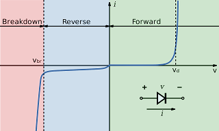
direction to the junction by the positive voltage. the V-I characteristics of PN Junction Diode is shown in below.
Important points on PN Junction Diode
1.
Semiconductors
have two types of mobile charge carriers, “Holes”
& “Electrons”.
2.
The
holes are (+Ve) positively charged
while the electrons (-Ve) negatively
charged particles.
3.
N-type semiconductor is doped with donor
impurities such as (phosphorus) P, As (Arsenic), Sb (antimony)
etc… so that it contains mobile charges
which are electrons.
4.
Practically Barrier Potential of PN-Junction Diode is 0.5 To 1 Micron (106).
5.
Barrier potential width of PN-Junction Diode is depends is depends on the temperature .when temperature increases potential barrier width is
decreased
6.
Reverse saturation current (I0)
of PN-Junction Diode is doubles for every 100
rise for germanium and for every 60
rise in silicon.
7.
Barrier potential of PN-Junction Diode is decreased approximately 2.5 mv per degree rise in temperature.
8.
Barrier Potential of Is Depends On The Following
· Type Of Semi-Conductor
·
Donor
Impurity Added
·
Acceptor
Impurity Added
· Temperature
9.
A
P-type semiconductor is doped with acceptor impurities such as Boron, Aluminium so that it contains mobile charges
which are mainly holes.
10. The junction region of PN-Junction Diode which has no charge carriers is
known as the depletion region.
11. The depletion region of PN-Junction Diode has a physical thickness that
varies with the applied voltage.
12. When a diode is Zero Biased no external energy
source is applied and a natural Potential
Barrier is developed across a depletion layer which is
approximately 0.6V to 0.7V for
silicon diodes and approximately 0.3V
for germanium diodes.
13. When a junction diode is Forward Biased the thickness of
the depletion region reduces and the diode acts like a short circuit allowing
full current to flow.
14. When depletion region or space
charge region is more then it will acts as an Insulator
15. When a PN junction diode is Reverse Biased the width or thickness
of the depletion region is increases and the diode acts like an open circuit.


